

The Next Level of Efficiency in Chip Manufacturing Is Taking Shape Below the Cleanroom
News originally published by
EIN Presswire
Subfab NetZero by DAS Environmental Experts: Integrating emissions reduction, measurement and intelligent control for more efficient semiconductor manufacturing.
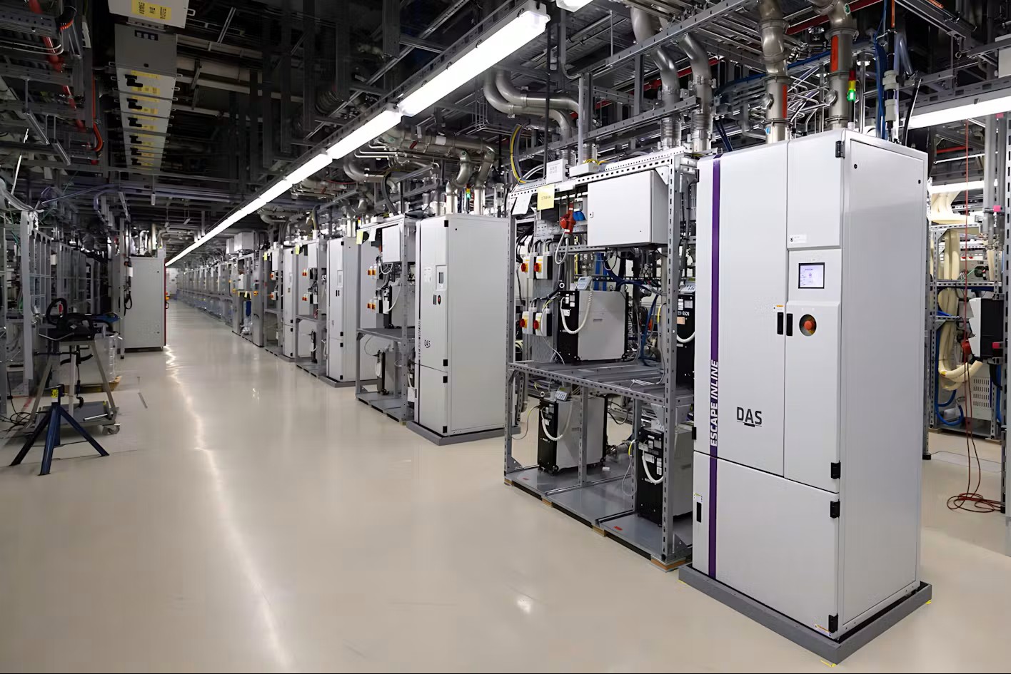
DAS Environmental Experts waste gas abatement systems installed in a semiconductor subfab, supporting emissions reduction in chip manufacturing.
Integrated approach combines waste gas abatement, emissions measurement and intelligent equipment control. New ALCEA system enables up to 95% NOx reduction.
DRESDEN, SAXONY, GERMANY, November 16, 2026 /EINPresswire.com/ -- **MUNICH/DRESDEN, GERMANY, November 10, 2026** – The semiconductor industry is investing billions in new production capacity while facing increasing pressure to reduce emissions, resource consumption and operating costs. One key area for improvement is the subfab, the technical infrastructure beneath the cleanroom.At SEMICON Europa, DAS Environmental Experts is unveiling **Subfab NetZero**, a holistic concept that connects waste gas abatement, emissions measurement, digital connectivity and intelligent equipment control. The company is also introducing **ALCEA**, a new system for reducing nitrogen oxide (NOx) emissions. Initial discussions with semiconductor manufacturers about potential applications of Subfab NetZero are already underway.
**The Subfab: A Key Lever for Environmental Performance**
The subfab houses vacuum pumps, waste gas abatement systems and other equipment essential to semiconductor manufacturing. These systems significantly influence energy consumption, the use of gases, water and chemicals, and overall emissions.
Although individual technologies have become increasingly efficient, DAS Environmental Experts sees further potential in connecting manufacturing processes and subfab infrastructure more closely.
Three developments are accelerating this shift: rising costs for energy and resources, increasing requirements for measurable environmental improvements, and growing demand for reliable operating data. Advances in sensors, emissions monitoring and digital connectivity now make it possible to better coordinate previously isolated equipment systems.
“The semiconductor industry has made enormous progress in treating waste gases. The next opportunity lies in gaining a better understanding of the environmental performance of the entire subfab and managing its operation more intelligently. If we continuously capture emissions and operating states and run the equipment accordingly, we can improve environmental performance and resource efficiency in tandem. That is precisely the approach we are pursuing with Subfab NetZero,” says **Dr. Guy Davies, Chief Business Development Officer at DAS Environmental Experts**.
**Subfab NetZero: Connecting Technologies for Greater Efficiency**
Subfab NetZero combines established waste gas treatment technologies with new capabilities in emissions measurement, digital connectivity and intelligent operational optimization.
The concept follows a closed control loop comprising four functions: **Abate, Measure, Validate and Optimize**.
By continuously capturing relevant emissions and equipment operating states wherever technically feasible, the approach aims to enable demand-based system control, reduce unnecessary resource consumption and verify environmental improvements through measurement data.
Rather than optimizing individual systems in isolation, the objective is to improve the environmental performance of the entire subfab through coordinated operation.
The concept builds on more than three decades of DAS experience in waste gas treatment, complemented by ongoing developments in environmental validation, digital interfaces and AI-assisted data analysis.
Subfab NetZero represents a long-term technological transformation approach rather than a single product or immediately deployable solution.
**ALCEA: Up to 95% NOx Reduction Without Additional Floor Space**
The new ALCEA system demonstrates how DAS Environmental Experts is expanding its technology portfolio to support more comprehensive emissions reduction. SEMICON Europa marks its European trade show debut.
ALCEA provides secondary treatment of nitrogen oxides generated by upstream waste gas abatement systems. It can be installed directly in existing exhaust ducts, making it suitable for retrofitting without requiring additional floor space in the subfab.
Under specified operating conditions, ALCEA achieves **up to 95% NOx reduction**. The technology complements existing waste gas treatment systems and addresses the growing need to reduce emissions while limiting additional infrastructure and utility requirements.
Its compact integration illustrates an important principle behind Subfab NetZero: environmental performance must be improved without unnecessarily increasing the complexity or resource consumption of semiconductor manufacturing.
**Intelligent Control Reduces Resource Consumption and Costs**
Existing DAS technologies already demonstrate the potential of adapting waste gas treatment to actual process requirements.
One example is **Active Tool Coupling (ATC)**, which adjusts abatement system operation according to the operating state of connected semiconductor process tools.
In a documented application involving a four-chamber etch tool and an inline scrubber at a European semiconductor fab, ATC reduced fuel gas consumption by approximately **68% compared with continuous operation**. Additional savings in oxygen, compressed air and water consumption were also achieved.
These results demonstrate how demand-based control can improve resource efficiency while maintaining the required abatement performance.
The savings were measured under specific operating conditions and cannot be directly extrapolated to other installations or the entire subfab.
Nevertheless, the application illustrates the potential of closer coordination between manufacturing equipment and environmental technologies.
Subfab NetZero aims to extend this principle by combining operating data, emissions measurement and intelligent control within a broader optimization framework.
**First Semiconductor Manufacturers Exploring Applications**
DAS Environmental Experts is already discussing potential Subfab NetZero applications with an initial group of semiconductor manufacturers.
These discussions indicate interest in integrating emissions reduction, resource efficiency and intelligent equipment control more closely, rather than addressing each challenge separately.
Beginning in 2027, DAS plans to introduce the concept progressively in Asia and North America. Together with fab operators, the company intends to evaluate technological and economic opportunities at individual manufacturing sites.
Both existing facilities and new semiconductor fabs will be considered, recognizing that infrastructure, production technologies and environmental requirements vary considerably between locations. The transformation toward lower-emission semiconductor manufacturing will therefore require site-specific approaches and measurable improvements over time.
With Subfab NetZero, DAS Environmental Experts aims to support semiconductor manufacturers in reducing emissions and resource consumption, optimizing operating costs and documenting environmental progress through reliable measurement data.
The objective is a more connected, resource-efficient and environmentally responsible subfab – built on measurable performance and continuous improvement.
Daniela Georgi
DAS Environmental Expert GmbH
+49 351 40494000
Legal Disclaimer:
EIN Presswire provides this news content "as is" without warranty of any kind. We do not accept any responsibility or liability for the accuracy, content, images, videos, licenses, completeness, legality, or reliability of the information contained in this article. If you have any complaints or copyright issues related to this article, kindly contact the author above.
